

Executive Overview
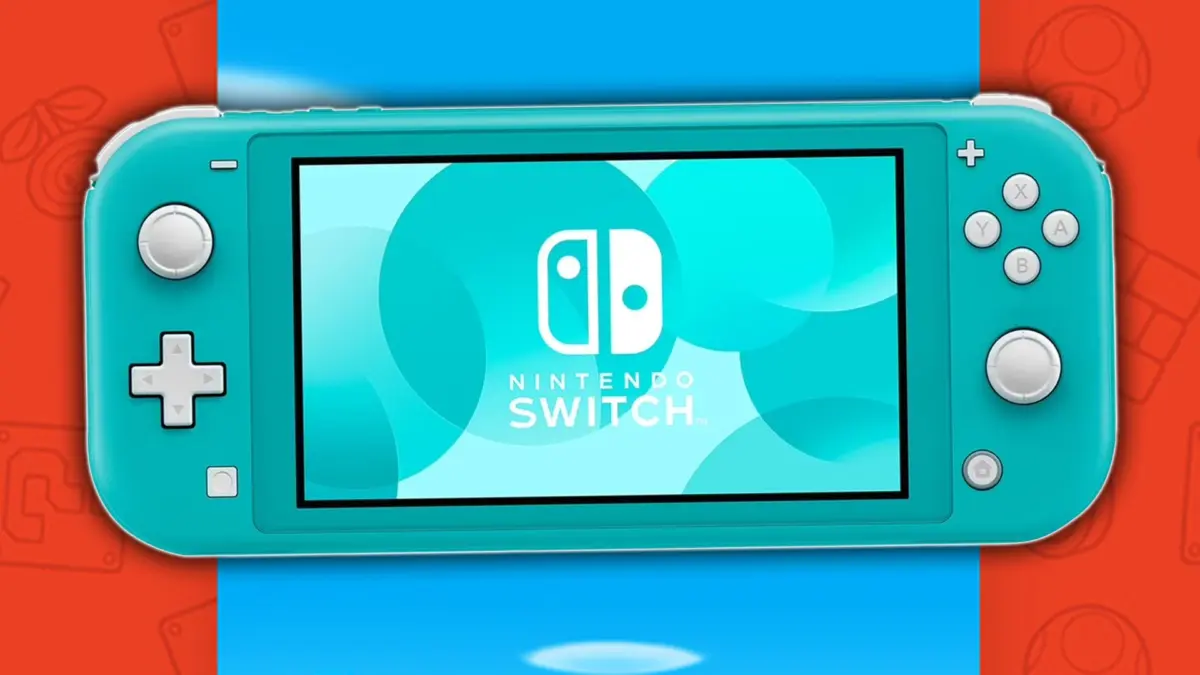
As the video game industry anticipates the arrival of Nintendo’s next-generation hardware—broadly designated by analysts and enthusiasts as the "Nintendo Switch 2"—industry supply chains are already dropping subtle clues regarding the platform’s long-term lifecycle strategy. While the primary flagship console is designed to retain the signature hybrid dockable architecture, emerging technical reports indicate that a streamlined, handheld-only variant—a conceptual "Switch 2 Lite"—may already be in the advanced planning stages.
Central to this speculation is a critical development in semiconductor manufacturing: Samsung Foundry’s upcoming second-generation 8LPU+ (Low Power Ultimate Plus) process node. Supply chain intelligence suggests that Nintendo and its long-standing silicon partner, Nvidia, could leverage this refined lithography process to create a smaller, highly power-efficient, and cost-effective system-on-chip (SoC).
By migrating from the standard 8nm/8LPU node—reportedly utilized for the primary Switch 2’s Nvidia Tegra T239 processor—to the refined 8LPU+ process, Nintendo would be positioned to produce a compact, budget-friendly handheld without sacrificing architectural feature parity. This strategic move mirrors Nintendo’s historical hardware iteration model, paving the way for a more accessible entry point into its next-generation gaming ecosystem.
Detailed Chronology of Hardware Speculation and Supply Leaks
The narrative surrounding Nintendo’s next-generation silicon has evolved over several years through a complex chain of data breaches, custom kernel commits, and semiconductor industry scheduling updates.
+-------------------------------------------------------------------+
|                     CHRONOLOGY OF EVENTS                          |
+-------------------------------------------------------------------+
|  MARCH 2022     | Nvidia Cyberattack Leaks                        |
|                 | - References to "NVN2" API and Tegra T239 SoC   |
|                 |   fabricated on Samsung's 8nm-class process.   |
+-----------------+-------------------------------------------------+
|  LATE 2023      | Supply Chain & Kernel Tracking                  |
|                 | - Shipping manifests reveal T239 testing boards; |
|                 |   Linux kernel commits confirm Ampere architecture.|
+-----------------+-------------------------------------------------+
|  OCTOBER 2026   | Korean Media Reports                            |
|                 | - Electronic Times highlights Samsung Foundry   |
|                 |   qualifications for the new 8LPU+ process node.|
+-----------------+-------------------------------------------------+
|  UPCOMING 2026  | Industry Standardization & Reveal               |
|                 | - Samsung scheduled to present 8LPU+ tech at    |
|                 |   the International Electron Devices Meeting.   |
+-----------------+-------------------------------------------------+
The Foundations: The Nvidia Tegra T239 Leak (2022)
The baseline architecture of Nintendo’s next console was first exposed during a high-profile cyberattack on Nvidia in early 2022. Leaked source code made explicit reference to "NVN2," a graphics Application Programming Interface (API) customized for Nintendo hardware, alongside references to a custom chip codenamed "Drake" or the Tegra T239. Built on Samsung’s custom 8nm-class manufacturing node, the T239 was identified as an octa-core ARM Cortex-A78AE processor paired with a custom GPU based on Nvidia’s Ampere architecture, featuring specialized hardware support for Deep Learning Super Sampling (DLSS) and Ray Tracing.
Supply Chain Manifests and Kernel Tracking (2023–2024)
Throughout 2023 and early 2024, international customs databases and Linux kernel commits corroborated the existence of the T239 processor. Logistics tracking showed sample shipments between Nvidia’s testing facilities and Nintendo’s assembly partners in East Asia. These manifests detailed test boards featuring custom power management integrated circuits (PMICs) and memory configurations designed specifically for a mobile form factor.
The Korean Industry Reports (October 2026)
The narrative shifted from the flagship console to mid-cycle hardware optimization when South Korean tech outlet Electronic Times (ETNews) published an investigation into Samsung Foundry’s operational roadmap. Citing unnamed industry sources, the report revealed that Samsung was preparing to roll out its enhanced 8LPU+ fabrication technology to existing high-volume clients. The report noted that custom chipmakers seeking low-cost, high-yield manufacturing options for handheld and mobile devices were actively evaluating the node for upcoming production runs.
Technical Validation: VideoCardz and IEDM 2026 Presentation
Building on the South Korean report, hardware authority VideoCardz linked Samsung’s publicly disclosed paper schedule for the 2026 IEEE International Electron Devices Meeting (IEDM) directly to potential custom gaming silicon. The presentation outlines the exact performance gains and physical spatial reductions offered by the 8LPU+ process over its predecessor, solidifying industry consensus that this node is engineered specifically to refresh and optimize mid-tier, high-volume mobile SoCs.
Technical Deep Dive: Supporting Context & Metrics
To understand why Samsung’s 8LPU+ process is a strong candidate for a revised "Switch 2 Lite" hardware revision, one must analyze the physical and economic demands of portable gaming hardware. Mobile gaming consoles exist within strict physical boundaries governed by thermal design power (TDP), battery size, and physical board area.
Comparative Node Performance Metrics
Samsung’s 8LPU+ process represents a second-generation refinement of its existing 8nm family, which itself evolved from earlier 10nm FinFET topologies. The technical specifications disclosed ahead of the 2026 IEDM highlight key physical optimizations:

| Metric / Specification | Standard Samsung 8LPU (Flagship SoC) | Advanced Samsung 8LPU+ (Lite Target Node) | Net Variance / Improvement |
|---|---|---|---|
| Logic Performance | Baseline Clock Frequencies | +12% Peak Clock Potential | +12% Performance |
| Power Consumption | Baseline Dynamic Power Draw | -15% at Equivalent Frequency | -15% Power Draw |
| Silicon Die Footprint | Baseline Area ($mm^2$) | 8% Footprint Reduction | -8% Total Die Size |
| I/O Circuitry Area | Baseline Input/Output Layout | ~10% Footprint Reduction | ~10% I/O Area Reduction |
| Standby Power Leakage | Baseline Transistor Leakage | Suppressed Off-State Current | Significant Reduction |
    PERFORMANCE & EFFICIENCY GAINS (8LPU vs. 8LPU+)

    Logic Performance     [|||||||||||||||||||||||||] +12%
    Power Consumption     [||||||||||||||||||||||] -15%
    Die Footprint Size    [||||||||||||] -8%
    I/O Circuitry Area    [||||||||||||||] -10%
                          0%   5%   10%  15%  20%
Engineering Implications for Handheld Hardware
1. Thermal Management and Clock Stability
A 15% reduction in dynamic power consumption directly lowers the thermal output of the SoC under peak load. In a compact, integrated handheld chassis—which lacks active cooling fans or relies on minimal, low-profile heatsinks—managing thermal throttling is critical. Reduced wattage requirements allow the custom Tegra chip to maintain target operating clock rates consistently without generating excess heat that could degrade battery life or uncomfortable external chassis temperatures.
2. Battery Life Optimization and Standby Power
Handheld devices are heavily judged on battery longevity during active gameplay and operational efficiency during sleep modes. The targeted suppression of standby transistor leakage in the 8LPU+ process means that a potential Switch 2 Lite would lose far less charge while suspended in sleep mode. On the go, the 15% efficiency gain directly extends operational runtime per milliamp-hour (mAh) of battery capacity, allowing Nintendo to downsize the battery cell to save weight and physical volume without reducing play sessions.
3. Silicon Economics and Manufacturing Yields
The economic argument for 8LPU+ is compelling. An 8% overall die area reduction, combined with a 10% decrease in input/output (I/O) physical circuitry, yields significantly more functional dies per silicon wafer. In semiconductor manufacturing, smaller die sizes directly translate to higher wafer yield rates and lower cost-per-unit production. For a commercial product designed to hit an entry-level price point, every fractional dollar saved on SoC fabrication improves retail profit margins.
Historical Precedents: Nintendo’s Hardware Iteration Strategy
Nintendo’s potential deployment of a revised silicon process for a budget-focused console revision aligns directly with its established business practices across multiple console generations.
     HISTORICAL HARDWARE REVISION STRATEGY

     2017: Original Nintendo Switch
           ↳ NVIDIA Tegra X1 (20nm TSMC Process)

     2019: Switch "Mariko" Refresh & Switch Lite
           ↳ NVIDIA Tegra X1+ (16nm FinFET Process)
           ↳ Outcome: +40-50% Battery Life / Smaller Form Factor

     FUTURE: Nintendo Switch 2 Platform
           ↳ Base Model: Custom Tegra T239 (Samsung 8LPU)
           ↳ Lite Revision: Refined Tegra T239 (Samsung 8LPU+)
The 2019 "Mariko" Revision (Tegra X1 to Tegra X1+)
When Nintendo launched the original Switch in 2017, the console ran on an Nvidia Tegra X1 processor manufactured on TSMC’s 20nm process node. By 2019, Nintendo quietly transitioned the platform to the "Mariko" revision of the chip (the Tegra X1+), fabricated on TSMC’s enhanced 16nm FinFET process.
This node shrink yielded massive efficiency gains:
- The Standalone Switch Lite (2019): Enabled Nintendo to drop docking hardware, eliminate detachable Joy-Cons, shrink the battery, and sell a purely portable device for $199 while maintaining reasonable battery life.
- The "Red Box" Switch Refresh (2019) & OLED Model (2021): Extended battery life from 2.5–6.5 hours to 4.5–9.0 hours using the exact same battery capacity, purely through silicon process efficiency gains.
Portable Platform Refinements
The historical trajectory extends back decades:
- Game Boy to Game Boy Pocket (1996): Reduced battery requirement from four AA batteries to two AAA batteries through board integration and screen power reductions.
- Nintendo DS to Nintendo DS Lite (2006): Scaled down screen power requirements, increased display brightness, and shrunk the total hardware volume by 39%.
- Nintendo 3DS to 2DS / New 2DS XL: Streamlined internal components, stripped tertiary features (like autostereoscopic 3D), and consolidated processing silicon to establish a budget-friendly platform for younger audiences.
Official Statements, Corporate Silence, and Industry Analysis
As is standard practice for major hardware manufacturers, official communications remain tightly guarded, requiring industry analysts to read between the lines of supply chain disclosures and corporate presentations.
Nintendo’s Corporate Stance
Nintendo maintains a strict policy of refusing to comment on rumors, hardware leaks, or prospective product roadmaps. During quarterly financial results briefings, company leadership consistently emphasizes that research and development efforts are continuous, but new hardware variants are only announced when production, software support, and distribution networks are fully aligned.
Semiconductor Industry Analysis
Commenting on the broader strategic implications of Samsung’s 8LPU+ node, mobile platform analysts emphasize that mature, optimized node iterations are vital for sustaining consumer electronics lifecycles.

"When advanced nodes like 3nm and 2nm capture headlines for premium smartphones, refined legacy nodes—such as Samsung’s 8LPU+—become the operational workhorses of the industry," notes a senior supply chain analyst specializing in East Asian foundries. "For high-volume consumer platforms where retail pricing is sensitive, moving to an optimized, mature process node provides the perfect balance of yield reliability, lower manufacturing cost, and meaningful thermal improvements."
Samsung Foundry’s Position
Samsung Foundry’s disclosure regarding 8LPU+ at the upcoming International Electron Devices Meeting (IEDM) demonstrates a commercial strategy aimed at retaining high-volume fab clients. Facing intense competition from TSMC in the leading-edge sub-3nm market, Samsung has strategically focused on optimizing its 8nm and 5nm nodes to offer cost-conscious hardware designers a compelling alternative to more expensive lithography options.
Future Outlook and Strategic Market Impact
The prospective emergence of a Samsung 8LPU+-powered "Nintendo Switch 2 Lite" carries significant strategic implications for the handheld gaming market over the next three to five years.
+-----------------------------------------------------------------------+
|                    NEXT-GEN PORTABLE LANDSCAPE                        |
+-----------------------------------------------------------------------+
|  ENTRY LEVEL ($199–$249)    | MID-RANGE ($399–$499) | HIGH END ($699+) |
+-----------------------------+-----------------------+-----------------+
|  • Switch 2 Lite            | • Flagship Switch 2   | • PC Handhelds  |
|    (Dedicated Handheld)     |   (Hybrid Console)    |   (ROG Ally,    |
|  • Optimized 8LPU+ Silicon  | • Standard 8LPU SoC   |   Steam Deck)   |
|  • Maximum Portability      | • DLSS Docking Target | • High Power    |
+-----------------------------+-----------------------+-----------------+
Market Segmentation and Consumer Pricing
The flagship Nintendo Switch 2 is widely expected to enter the market at a higher price point than its 2017 predecessor, driven by broader inflation, more complex computational components, higher memory configurations, and advanced features like DLSS support.
A future Switch 2 Lite, launched 18 to 24 months into the generation, would serve as Nintendo’s essential market expansion tool:
- Entry-Level Accessibility: A targeted price point (potentially $199 to $249) ensures access for families, younger players, and multi-console households.
- Ecosystem Retention: Ensures that demanding next-generation titles remain playable across the entire hardware family without splitting the software user base.
Competitive Handheld Landscape
The handheld market today is drastically different from the market of 2017 or 2019. The rise of x86 handheld gaming PCs—such as Valve’s Steam Deck, ASUSTOR/ASUS ROG Ally, and Lenovo Legion Go—has established a thriving market for high-performance mobile gaming. However, these x86 devices often suffer from high price tags, short battery lifespans, and substantial physical bulk.
By pairing Nvidia’s optimized Ampere architecture with Samsung’s efficient 8LPU+ fabrication, Nintendo can offer a custom ARM-based platform that delivers exceptional performance per watt. This hardware optimization allows Nintendo to deliver smooth performance and native software optimization in a lightweight, accessible handheld form factor that general-purpose PC hardware struggles to replicate at a lower price point.
Timeline Expectations
Given that Samsung is set to formally present the technical specifications of its 8LPU+ node at the 2026 IEDM session, high-volume commercial production utilizing this lithography process is unlikely to peak before late 2026 or early 2027. Consequently, while the standard hybrid Nintendo Switch 2 will establish the initial generation, players seeking a streamlined, budget-focused handheld variant will likely see a Switch 2 Lite hit the global market during the secondary phase of the hardware cycle—built quietly upon Samsung’s refined silicon foundation.







Belum ada komentar. Jadilah yang pertama berkomentar!